:: DIY thermal envelop designing for 5x5cm PCB
sub part in getting the thermal envelops right on track literally.
parts in use
1) PNP BJT DPAK MJD45H11T4G, R-jc = 6.25˚C/w , R-ja = 71.4˚C/w , max p = 20w, max t-op = 150˚C
2) PMOS DPAK SUD50P04-08-GE3, R-jc = 1.7˚C/w , R-ja = 50˚C/w , max p = 75.5w, max t-op = 150˚C
3) heatsink : 116mm x 60mm x 22mm. 16fins x 20mm x 60mm x 1.5mm. nominal 2.2˚C/watt @ emissivity = 0.9, with generic forced air of 300LFM = 0.88˚C/watt
4) DPAK PCB pads, 85x vias 0.6mm PCB = 1.39˚C/w (pad size 8.9x8.9mm / 350mils)
item1 :
thermal calculation max imposed operating temperature Tj = 140˚C, R-jc = 6.25˚C/w, R-cs = 0.1˚C/w R-pcb = 1.39˚C/w and R-sa = 0.88˚C/w (ambient temperature = 30˚C). total power envelop of this setup is 110/8.62 = 12.76watts. heatsink temperature = 12.76 x 0.88 + 30 = 41.23˚C
item2 :
thermal calculation max imposed operating temperature Tj = 140˚C, R-jc = 1.7˚C/w, R-cs = 0.1˚C/w R-pcb = 1.39˚C/w and R-sa = 0.88˚C/w (ambient temperature = 30˚C). total power envelop of this setup is 110/4.07 = 27.03watts. heatsink temperature = 27.03 x 0.88 + 30 = 53.79˚C
summing up the output power 4 PNP BJT will dissipate 50.8w, while 2 PMOS dissipates 54.06w.
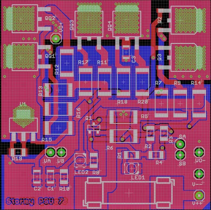
at board level, actual vias :
Tj = 140˚C, R-jc = 6.25˚C/w, R-cs = 0.1˚C/w (R-pcb = 118/78 = 1.51 ˚C/w) and R-sa = 0.88˚C/w (ambient temperature = 30˚C). total power envelop of this setup is 110/8.74 = 12.59watts. heatsink temperature = 12.76 x 0.88 + 30 = 41.08˚C
Tj = 140˚C, R-jc = 1.7˚C/w, R-cs = 0.1˚C/w R-pcb = 1.51˚C/w and R-sa = 0.88˚C/w (ambient temperature = 30˚C). total power envelop of this setup is 110/4.19 = 26.25watts. heatsink temperature = 27.03 x 0.88 + 30 = 53.10˚C.
the further i evolve the circuit, the further i evolve its operation envelope ...


Comments
Post a Comment
feel free to ask me anything