:: the idea of fully using SMD power devices
well as some of you electronics hobbyists know, due to certain
design limitations or geographical disadvantages, we may not have
full large package power devices to implement (eg : TO-247 ?) or
maybe there is a sale going on and for the cost of a single TO-247,
the equivalent DPAK would get you say 10 units. Or maybe, for
circuitry redundancy issues, you just have to fit in the smaller
SMDs.
take for a scenario, logic level drive MOSFET, use in ESC, very small package required, very high current draw. we prolly want to look at something like PSMN1R5-30YL, 30v VDS, theoretical 44A sustained loading with a 3w dissipation. max frequency theoretical 380kHz. about SGD$1.50, stock about 1000 left. if the motor is drawing over 20A sustained, for 1:4 safety, they could implement 2 of those MOSFETS.
take for a scenario, logic level drive MOSFET, use in ESC, very small package required, very high current draw. we prolly want to look at something like PSMN1R5-30YL, 30v VDS, theoretical 44A sustained loading with a 3w dissipation. max frequency theoretical 380kHz. about SGD$1.50, stock about 1000 left. if the motor is drawing over 20A sustained, for 1:4 safety, they could implement 2 of those MOSFETS.
So I have been toying with the idea of extending the power
handling capabilities of power SMD devices. As with all traditional
heat sinking issues, the chunkier the sinking, the better it is. As I
have experimented with some very basic PCB based heat spreading
techniques, they just do not add up the total number of watts (on
first glance).
So the next step will be to move the SMD package right onto the
heatsink it self. Unlike TO-247 packages where they have a built in
mechanical fastening hole to improve thermal conductivity, the SMD
will need a small mod. Using a brass intermediary piece, the SMD
solders onto this hot seat which has mechanical fastening holes, and
then it gets the bolt-on direct to heatsink. While brass may not be
the perfect heatsinking material, it is what I could grab readily at
the local craft store, and it seems to be very much cheaper than
copper in the small quantities presented. There are of course larger
hardware stores where copper could be gotten for cheaper, but I
prolly will need to buy in hundreds of kilos which in that case, I
will prolly go crazy over storage.
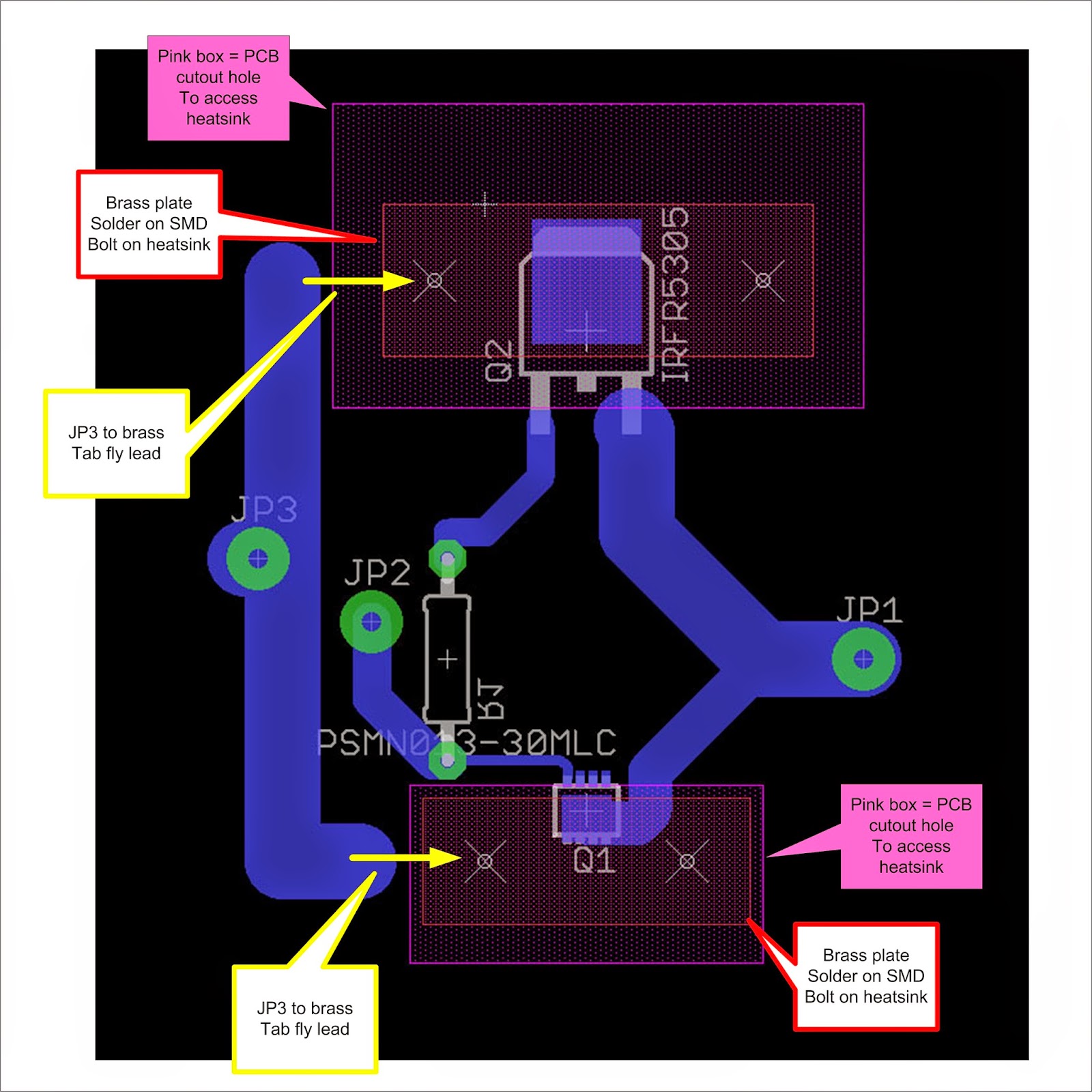
Here we see a mock up PCB trace, there is the 2 tiny power SMDs, the common DPAK and the not so common LFPAK33. Like
normal TO-247 kind of PCB where the board will bolt onto a backing
heatsink and a cutout is where the package will pop right onto the
heat sink block, the same is happening here except the cutout would
likely be bigger to accommodate the brass piece and probably 2
screws (the tab connection will likely be a short fly lead). In this fashion, it will also be possible for the SMD package
to have electrical isolation from the sink just like the larger
packages with the right mechanical fixtures (plastic screw washers,
mica plates, thermal grease, silicone pads, etc). As I have yet to
try this setup, I will post more updates in later tests.
in professional capacities, larger commercial entities will opt for heavy copper plated PCBs. in hobby or probably budget capacity, i think this will be a very good way forward to solve heat dissipation issues.
However the extra challenge presented here would be the soldering of the package to the brass piece. most packages denote a 260 degree C 10second exposure limit. it will be very challenging to keep to this working limitation. most handheld soldering irons are going off with at least 300degrees heat. it will be best to use a controlled reflow oven or a very good hot air gun.


Comments
Post a Comment
feel free to ask me anything